Recently, Samsung held the Samsung Foundry Factory Forum (SFF) 2018 meeting in Japan and updated the technology roadmap.
In short, there are three main points to discuss. First, the 7nm process technology based on EUV technology will be mass-produced in the next few quarters (initial EUV is only used to select layers), the second is to introduce 8nm LPU process, and the third is to reiterate. Around the 3nm node, a Gate-all-around FET (GAAFET) will be introduced to replace the FinFET (Fin Field Effect Transistor).
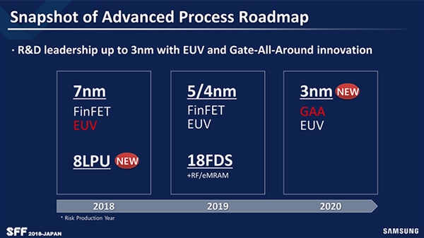
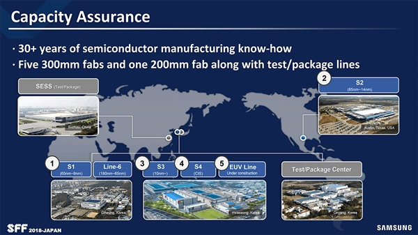
Regarding the first point, Samsung said that it has deployed several ASML Twinscan NXE:3400B EUV lithography machines at the S3 plant in Hwaseong, South Korea. The new EUV production line with an investment of 6 trillion won is expected to be completed in 2019 and expand production in 2020.
At present, the official 7-inch LPP process is the Qualcomm Snapdragon 5G SoC.
Regarding the second point, 8LPU (low power ultimate) is a modified version of 8LPP, which reduces the chip area and 10% power consumption by 10% compared with 10LPP. It seems that LPU will further make a fuss about power consumption and area…
As Samsung’s 7LPP replenishment capacity needs to wait until 2020, this is the opportunity for 8LPU to make a big impact in the market. According to ZDNet, Qualcomm is also a Samsung’s 8LPU customer.
As for the third point, Samsung will use the limits of FinFET technology to 5LPE and 4LPP and plan to risk trial production in 2019. However, in the 3nm era, the chip is getting smaller and smaller, the current channel width is narrowing, and it is difficult to control the current direction. Samsung has proposed a GAAFET solution, which is scheduled to be trial-produced in early 2020.
In addition, Samsung also said that in 2019, single-chip packaging technology 3D SiP will be ready.
Related Posts
Samsung Galaxy S24 Series Rumors: Release Date and What to Expect
Samsung Galaxy Z Flip 5 debuts in yellow color! Know all about it
Expected release of the new Samsung Galaxy Ring by the end of 2024 or early 2025
Samsung to reportedly add cloud gaming service to Galaxy phones
Galaxy Z Fold 5 vs. Galaxy Z Fold 4 – Should you Upgrade?
Samsung Galaxy Tab S9 Series – Price and Specifications Revealed