Samsung official website announced that Samsung Electronics has successfully completed the development of 5nm EUV to achieve larger area expansion of the chip and bring ultra-low power consumption.
Samsung Electronics said that the development of its 5 nanometer (nm) FinFET process technology has been completed and can now provide samples for customers. By adding another cutting-edge node to its ultra-UV (EUV)-based process products, Samsung claims once again demonstrates its leadership in the advanced foundry market.
Compared to 7nm, Samsung’s 5nm FinFET process technology increases logic area efficiency by 25%, power consumption by 20%, and performance by 10%, enabling more innovative standard cell architectures.
Samsung said that another major advantage of 5nm is that it can reuse all 7nm intellectual property (IP) to 5nm. As a result, the 7nm customer transition to 5nm will greatly benefit from reduced migration costs, pre-validated design ecosystems, and thus shorten their 5nm product development time.
In the recently published Samsung press release: “Successfully completed 5nm development, we have proven our capabilities in EUV-based nodes,” said Charlie Bae, executive vice president of Samsung Electronics’ foundry business. “In response to our customers’ growing demand for advanced process technologies to differentiate their next-generation products, we continue to accelerate the mass production of EUV-based technologies.”
In October 2018, Samsung announced the preparation and preliminary production of the 7nm process, which is its first process node using EUV lithography. The company has provided commercial samples of the industry’s first new EUV-based products and began mass production of the 7nm process earlier this year.
In addition, Samsung is working with 6nm customers, a custom EUV-based process node, and has received its first 6nm chip.
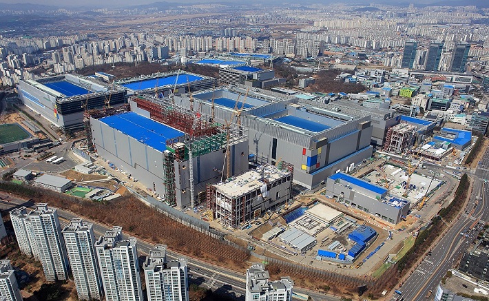
The EUV-based process technology of the Samsung foundry is currently being produced on the S3 line in Hwaseong, South Korea. In addition, Samsung will expand its EUV capacity to Hwaseong’s new EUV production line, which is expected to be completed in the second half of 2019 and will start production next year.
Related Posts
Samsung Galaxy S24 Series Rumors: Release Date and What to Expect
Samsung Galaxy Z Flip 5 debuts in yellow color! Know all about it
Expected release of the new Samsung Galaxy Ring by the end of 2024 or early 2025
Samsung to reportedly add cloud gaming service to Galaxy phones
Galaxy Z Fold 5 vs. Galaxy Z Fold 4 – Should you Upgrade?
Samsung Galaxy Tab S9 Series – Price and Specifications Revealed